Photo sent by Alexander (Allroy), Novorossiysk
By chance, I got a "modernized" power amplifier "Oda-UM102S". The modernization was carried out by an unknown master so severely that only good "meaty" radiators survived. So I decided to adapt my new project to them, which flowed smoothly due to the desire to try out a new idea in hardware.
 History reference
The stereophonic radio complex "Oda 102 Stereo" since 1986 has been producing the Murom plant "RIP". The complex provided reception of mono and stereo transmissions in the VHF range, recording of mono and stereo programs, followed by playback. The complex consisted of 5 functionally completed units: an Oda-102S VHF tuner, an Oda-302S cassette recorder, an Oda UM-102S power amplifier, an Oda UP-102S preamplifier and 2 acoustic systems "15AC-213".
Excluded fragment. Our magazine exists on donations from readers. The full version of this article is only available
How to make L1 i, but if this option bothers anyone, then the coil can be wound on a 2-watt 10-33 Ohm resistor with a wire with a diameter of 0.8 mm in one layer.
VT5, VT6 are equipped with small radiators, which are aluminum plate 10x20 mm.
--
Thanks for attention!
Igor Kotov, editor-in-chief of Datagor magazine
Thanks for attention!
Andrey Zelenin,
Kyrgyzstan, Bishkek
Figure 1 The LANZAR power amplifier circuit is completely based on bipolar transistors.
INCREASE

Figure 2 LANZAR power amplifier circuit using field-effect transistors in the penultimate stage.
INCREASE

Figure 3 Schematic of the LANZAR power amplifier from the MS-8 simulator. INCREASE
|
LIST OF ELEMENTS INSTALLED IN THE LANZAR AMPLIFIER |
|
|
FOR BIPOLAR VERSION |
FOR THE OPTION WITH FIELD WORKERS |
| C3,C2 = 2 x 22µ0 C4 = 1 x 470p C6,C7 = 2 x 470µ0 x 25V C5,C8 = 2 x 0µ33 C11,C9 = 2 x 47µ0 C12,C13,C18 = 3 x 47p C15,C17,C1,C10 = 4 x 1µ0 C21 = 1 x 0µ15 C19,C20 = 2 x 470µ0 x 100V C14,C16 = 2 x 220µ0 x 100V R1 = 1 x 27k VD1,VD2 = 2 x 15V VT2,VT4 = 2 x 2N5401 |
C3,C2 = 2 x 22µ0 C4 = 1 x 470p C6,C7 = 2 x 470µ0 x 25V C5,C8 = 2 x 0µ33 C11,C10 = 2 x 47µ0 C12,C13,C18 = 3 x 47p C15,C17,C1,C9 = 4 x 1µ0 C21 = 1 x 0µ15 C19,C20 = 2 x 470µ0 x 100V C14,C16 = 2 x 220µ0 x 100V R1 = 1 x 27k VD1,VD2 = 2 x 15V VT8 = 1 x IRF640 |
For example, let's take the supply voltage equal to ±60 V. If the installation is done correctly and there are no faulty parts, then we will get a voltage map shown in Figure 7. The currents flowing through the elements of the power amplifier are shown in Figure 8. The dissipated power of each element is shown in Figure 9 (on transistors VT5, VT6, about 990 mW is dissipated, therefore, the TO-126 package requires a heat sink).

Figure 7. LANZAR power amplifier voltage map ENLARGE

Figure 8. Power Amplifier Current Map ENLARGE

Figure 9. Amplifier power dissipation map
A few words about the details and installation:
First of all, you should pay attention to the correct installation of parts, since the circuit is symmetrical, errors are quite common. Figure 10 shows the layout of the parts. The adjustment of the quiescent current (the current flowing through the terminal transistors with the input closed to a common wire and compensating the current-voltage characteristic of the transistors) is performed by resistor X1. When you first turn on the resistor slider must be in the upper position according to the diagram, i.e. have maximum resistance.
Quiescent current should be 30...60 mA. There is no point in putting it higher - neither the instruments nor the tangible changes occur by ear. To set the quiescent current, the voltage is measured at any of the emitter resistors of the final stage and is set in accordance with the table:
|
VOLTAGE AT THE OUTPUTS OF THE EMITTER RESISTOR, V |
QUIET CURRENT TOO LOW, STEP DISTORTION POSSIBLE, NORMAL QUIET CURRENT, HIGH QUIET CURRENT - EXCESSIVE HEATING, IF THIS IS NOT AN ATTEMPT TO CREATE A CLASS "A", THEN THIS IS EMERGENCY CURRENT. | |||||
|
QUIET CURRENT OF ONE PAIR OF FINAL TRANSISTORS, mA |
||||||
|
|
|
|
||||
|
|
|
|
||||

Figure 10 Location of parts on the power amplifier board. Shown are the places where the most common installation errors occur.
The question was raised about the advisability of using ceramic resistors in the emitter circuits of terminal transistors. You can also use MLT-2, two pieces connected in parallel with a nominal value of 0.47 ... 0.68 Ohm. However, the distortions introduced by ceramic resistors are too small, but the fact that they are interrupted - when overloaded, they break off, i.e. their resistance becomes infinite, which quite often leads to the rescue of terminal transistors in critical situations.
The area of the radiator depends on the cooling conditions, Figure 11 shows one of the options, it is necessary to fasten the power transistors to the heat sink through insulating gaskets
. It is better to use mica, since it has a rather small thermal resistance. One of the options for mounting transistors is shown in Figure 12.

Figure 11 One of the radiator options for a power of 300 W, subject to good ventilation

Figure 12 One of the options for mounting power amplifier transistors to a heatsink.
Insulating pads must be used.
Before mounting power transistors, as well as in case of suspicion of their breakdown, power transistors are checked by a tester. The limit on the tester is set to test the diodes (Fig. 13).

Figure 13 Checking the terminal transistors of the amplifier before installation and in case of suspicion of breakdown of transistors after critical situations.
Is it worth it to select transistors for coffee. amplification? There are quite a lot of disputes on this topic and the idea of selecting elements has been going on since the deep seventies, when the quality of the element base left much to be desired. Today, the manufacturer guarantees the spread of parameters between transistors of one batch of no more than 2%, which in itself speaks of the good quality of the elements. In addition, given that the terminal transistors 2SA1943 - 2SC5200 are firmly established in sound engineering, the manufacturer began to produce paired transistors, i.e. both direct and reverse conduction transistors already have the same parameters, i.e. the difference is not more than 2% (Fig. 14). Unfortunately, such pairs are not always found on sale, however, several times we happened to buy "twins". However, even having a parsing of coffee. gain between transistors of direct and reverse conduction, it is only necessary to ensure that transistors of the same structure are of the same batch, since they are connected in parallel and the spread in h21 can cause an overload of one of the transistors (for which this parameter is higher) and, as a result, overheating and exit from building. Well, the spread between transistors for positive and negative half-waves is fully compensated by negative feedback.
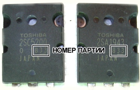
Figure 14 Transistors of different structures, but of the same batch.
The same applies to differential stage transistors - if they are of the same batch, i.e. purchased at the same time in the same place, the chance that the difference in parameters will be more than 5% is VERY small. Personally, we prefer FAIRCHALD transistors 2N5551 - 2N5401, however, STs sound quite decent.
However, this amplifier is also assembled on the domestic element base. This is quite real, but let's make an adjustment for the fact that the parameters of the purchased KT817 and found on the shelves in my workshop, bought back in the 90s, will differ quite a lot. Therefore, here it is better to use the h21 meter available in almost all digital testers. True, this lotion in the tester shows the truth only for low power transistors. It will not be entirely correct to select the transistors of the final stage with its help, since h21 also depends on the current flowing. That is why separate test benches are already being made to reject power transistors. from adjustable collector currents of the tested transistor (Fig. 15). The calibration of a permanent device for rejecting transistors is carried out in such a way that the microammeter deviates half the scale at a collector current of 1 A, and completely at a current of 2 A. When assembling an amplifier only for yourself, you don’t have to make a stand; two multimeters with a current measurement limit of at least 5 A are enough.
To produce a rejection, you should take any transistor from the rejected batch and set the collector current to 0.4 ... 0.6 A for the penultimate stage transistors and 1 ... 1.3 A for the final stage transistors with a variable resistor. Well, then everything is simple - transistors are connected to the terminals and, according to the readings of the ammeter included in the collector, transistors with the same readings are selected, not forgetting to look at the readings of the ammeter in the base circuit - they should also be similar. A spread of 5% is quite acceptable; for dial indicators on the scale, you can make marks of the "green corridor" during calibration. It should be noted that such currents do not cause bad heating of the transistor crystal, and given that it is without a heat sink, the duration of measurements should not be stretched in time - the SB1 button should not be held down for more than 1 ... 1.5 seconds. Such a rejection will, first of all, allow you to select transistors with a really similar gain coefficient, and checking powerful transistors with a digital multimeter is only a check to calm your conscience - in the microcurrent mode, powerful transistors have a gain coefficient of more than 500, and even a small spread when checking with a multimeter in real current modes can turn out to be huge . In other words, when checking the gain coff of a powerful transistor, the multimeter reading is nothing more than an abstract value that has nothing to do with the transistor gain coff through the collector-emitter junction, at least 0.5 A flows.

Figure 15 Rejection of powerful transistors by gain coefficient.
Feed-through capacitors C1-C3, C9-C11 are not quite typical inclusion, in comparison with the factory analogues of amplifiers. This is due to the fact that with this inclusion, it is not a polar capacitor of a rather large capacity that is obtained, but the use of a 1 μF film capacitor compensates for the not entirely correct operation of electrolytes at high frequencies. In other words, this implementation allowed for a more pleasant sounding amplifier, compared to a single electrolyte or a single film capacitor.
In older versions of Lanzar, instead of diodes VD3, VD4, 10 ohm resistors were used. The change in the element base allowed us to slightly improve the performance at signal peaks. For a more detailed consideration of this issue, let's turn to Figure 3.
In the circuit, not an ideal power source is modeled, but closer to the real one, which has its own resistance (R30, R31). When playing a sinusoidal signal, the voltage on the power rails will look like that shown in Figure 16. In this case, the capacitance of the power filter capacitors is 4700 uF, which is somewhat small. For normal operation of the amplifier, the capacitance of the power supply capacitors must be at least 10,000 microfarads per channel, it is possible and more, but a significant difference is no longer noticeable. But back to Figure 16. The blue line shows the voltage directly on the collectors of the final stage transistors, and the red line shows the supply voltage of the voltage amplifier if resistors are used instead of VD3, VD4. As can be seen from the figure, the supply voltage of the final stage has dipped from 60 V and is located between 58.3 V in the pause and 55.7 V at the peak of the sinusoidal signal. Due to the fact that the capacitor C14 not only becomes infected through the decoupling diode, but also discharges at the peaks of the signal, the power supply voltage of the amplifier takes the form of a red line in Figure 16 and fluctuates from 56 V to 57.5 V, i.e. it has a range of about 1.5 IN.

Figure 16 voltage waveform when using decoupling resistors.

Figure 17 The shape of the supply voltages on the terminal transistors and voltage amplifier
Replacing the resistors with diodes VD3 and VD4, we get the voltages shown in Figure 17. As can be seen from the figure, the amplitude of the ripples on the collectors of the terminal transistors has not changed much, but the supply voltage of the voltage amplifier has taken on a completely different look. First of all, the amplitude decreased from 1.5 V to 1 V; by about 0.5 V, while when using a resistor, the voltage at the peak of the signal sags by 1.2 V. In other words, by simply replacing the resistors with diodes, it was possible to reduce the supply ripple in the voltage amplifier by more than 2 times.
However, these are theoretical calculations. In practice, this replacement allows you to get "free" 4-5 watts, since the amplifier comes at a higher output voltage and reduces distortion at signal peaks.
After assembling the amplifier and adjusting the quiescent current, you should make sure that there is no constant voltage at the output of the power amplifier. If it is higher than 0.1 V, then this already definitely requires adjustment of the operating modes of the amplifier. In this case, the easiest way is to select a "supporting" resistor R1. For clarity, we give several options for this rating and show the changes in the constant voltage at the output of the amplifier in Figure 18.

Figure 18 Variation of the DC voltage at the output of the amplifier depending on the noman R1
Despite the fact that on the simulator the optimal constant voltage was obtained only at R1 equal to 8.2 kOhm, in real amplifiers this value is 15 kOhm ... 27 kOhm, depending on which manufacturer the VT1-VT4 differential stage transistors are used.
Perhaps it is worth saying a few words about the differences between power amplifiers completely on bipolar transistors and using field workers in the penultimate cascade. First of all, when using field-effect transistors, the output stage of the voltage amplifier is VERY heavily unloaded, since the gates of field-effect transistors have practically no active resistance - only the gate capacitance is a load. In this version, the amplifier circuitry begins to step on the heels of class A amplifiers, since the current flowing through the output stage of the voltage amplifier almost does not change over the entire range of output powers. An increase in the quiescent current of the penultimate stage operating on a floating load R18 and the base of emitter followers of powerful transistors also varies within small limits, which ultimately led to a rather noticeable decrease in THD. However, there is a fly in the ointment in this barrel of honey - the efficiency of the amplifier has decreased and the output power of the amplifier has decreased, due to the need to apply a voltage of more than 4 V to the gates of the field workers to open them (for a bipolar transistor, this parameter is 0.6 ... 0.7 V ). Figure 19 shows the peak of the sinusoidal signal of the amplifier, made on bipolar transistors (blue line) and field devices (red line) at the maximum amplitude of the output signal.

Figure 19 Change in the amplitude of the output signal when using different element base in the amplifier.
In other words, a decrease in THD by replacing field-effect transistors leads to a “shortage” of about 30 W, and a decrease in the THD level by about 2 times, so it’s up to everyone to decide exactly what to set.
It should also be remembered that the THD level also depends on the amplifier's own gain. In this amplifier gain coefficient depends on the values of resistors R25 and R13
(at the used ratings, the gain coefficient is almost 27 dB). Calculate gain factor in dB can be given by the formula Ku = 20 lg R25 / (R13 +1), where R13 and R25 - resistance in Ohms, 20 - multiplier, lg - decimal logarithm. If it is necessary to calculate the gain coefficient in times, then the formula takes the form Ku = R25 / (R13 + 1) . This calculation may be necessary when manufacturing a preamplifier and calculating the amplitude of the output signal in volts in order to exclude the operation of the power amplifier in the hard clipping mode.
Decreasing your own coffee. gain up to 21 dB (R13 = 910 ohms) leads to a decrease in the THD level by about 1.7 times with the same output signal amplitude (increased input voltage amplitude).
Well, now a few words about the most popular mistakes when assembling an amplifier yourself.
One of the most common mistakes is installation of 15 V zener diodes with incorrect polarity, i.e. these elements do not work in voltage stabilization mode, but like ordinary diodes. As a rule, such an error causes a constant voltage to appear at the output, and the polarity can be both positive and negative (more often negative). The voltage value is based between 15 and 30 V. In this case, no element is heated. Figure 20 shows the voltage map with incorrect installation of zener diodes, which was issued by the simulator. The erroneous items are highlighted in green.

Figure 20 Power amplifier voltage map with incorrectly soldered zener diodes.
The next popular mistake is mounting transistors upside down, i.e. when they confuse the collector and emitter in places. In this case, there is also constant tension, the absence of any signs of life. True, the reverse switching on of the differential cascade transistors can lead to their failure, but then how lucky. The voltage map for "inverted" inclusion is shown in Figure 21.

Figure 21 Voltage map with "inverted" switching on of differential stage transistors.
Often transistors 2N5551 and 2N5401 are confused, and they can also confuse the emitter with the collector. Figure 22 shows the voltage map of the amplifier with the "correct" mounting of the transistors interchanged, and in Figure 23, the transistors are not only swapped, but also turned upside down.

Figure 22 Transistors of the differential stage are interchanged.

Figure 23 Transistors of the differential stage are swapped, besides, the collector and emitter are swapped.
If the transistors are mixed up in places, and the emitter-collector is soldered correctly, then a small constant voltage is observed at the amplifier output, the quiescent current of the window transistors is regulated, but the sound is either completely absent, or at the level “it seems to be playing”. Before mounting the transistors soldered in this way on a board, they should be checked for operability. If the transistors are interchanged, and even the emitter-collector is interchanged, then the situation is already quite critical, since in this variant for differential stage transistors the polarity of the applied voltage is correct, but the operating modes are violated. In this embodiment, there is a strong heating of the terminal transistors (the current flowing through them is 2-4 A), a small constant voltage at the output and a barely audible sound.
It is rather problematic to confuse the pinout of the transistors of the last stage of the voltage amplifier when using transistors in the TO-220 package, but transistors in the TO-126 package are quite often soldered upside down, swapping the collector and emitter. In this embodiment, a highly distorted output signal is observed, poor regulation of the quiescent current, and no heating of the transistors of the last stage of the voltage amplifier. A more detailed voltage map for this power amplifier mounting option is shown in Figure 24.

Figure 24 The transistors of the last stage of the voltage amplifier are soldered upside down.
Sometimes the transistors of the last stage of the voltage amplifier are confused. In this case, there is a small constant voltage at the output of the amplifier, if there is a sound, it is very weak and with huge distortions, the quiescent current is only regulated upwards. An amplifier voltage map with such an error is shown in Figure 25.

Figure 25 Erroneous mounting of the transistors of the last stage of the voltage amplifier.
The penultimate cascade and terminal transistors in the amplifier are confused too rarely, so this option will not be considered.
Sometimes the amplifier fails, the most common reasons for this are overheating of the final transistors or overload. Insufficient heat sink area or poor thermal contact of the transistor flanges can lead to heating of the final transistor crystal to the temperature of mechanical destruction. Therefore, before the power amplifier is fully put into operation, it is necessary to make sure that the screws or self-tapping screws that fasten the terminals to the radiator are fully tightened, the insulating gaskets between the flanges of the transistors and the heat sink are well lubricated with thermal paste (we recommend the good old KPT-8), as well as the size of the gaskets over the size of the transistor by at least 3 mm on each side. If the heat sink area is insufficient, and there is simply no other, then you can use 12 V fans, which are used in computer technology. If the assembled amplifier is planned to operate only at above average powers (cafes, bars, etc.), then the cooler can be switched on for continuous operation, since it will still not be heard. If the amplifier is assembled for home use and will be operated at low power, then the operation of the cooler will already be audible, and there is no need for cooling - the radiator almost does not heat up. For such modes of operation, it is better to use controlled coolers. Several options for controlling the cooler are possible. The proposed options for controlling the coolers are based on the temperature control of the radiator and are switched on only when the radiator reaches a certain, controlled temperature. You can solve the problem of failure of window transistors either by installing additional overload protection, or by carefully mounting the wires going to the speaker system (for example, use oxygen-free wires to connect speakers to an amplifier, which, in addition to reduced active resistance, have increased insulation strength, resistant to shock and temperature ).
For example, consider several options for the failure of terminal transistors. Figure 26 shows a voltage map in the event that the reverse terminal transistors (2SC5200) go open, i.e. transitions are burnt out and have the maximum possible resistance. In this case, the amplifier retains its operating modes, the output remains close to zero, but the sound quality definitely wants better, since only one half-wave of the sinusoid is reproduced - negative (Fig. 27). The same will happen if the direct terminal transistors (2SA1943) break, only a positive half-wave will be reproduced.

Figure 26 Reverse terminal transistors burnt out to a break.

Figure 27 The signal at the output of the amplifier in the case when the 2SC5200 transistors burned out completely
Figure 27 is a voltage map in a situation where the terminals are out of order and have the lowest possible resistance, i.e. shorted. This variant of a malfunction drives the amplifier into VERY harsh conditions and further burning of the amplifier is limited only by the power source, since the current consumed at this moment can exceed 40 A. The surviving parts instantly gain temperature, in the arm where the transistors are still working, the voltage is slightly more than in where the short circuit to the power bus actually occurred. However, it is this situation that belongs to the easiest diagnostics - before turning on the amplifier, it will be enough to check the resistance of the transitions between each other with a multimeter, without even unsoldering them from the amplifier. The limit of the measurement set on the multimeter is DIOD TEST or BEEP. As a rule, burnt transistors show resistance between junctions in the range from 3 to 10 ohms.

Figure 27 Power amplifier voltage map in case of burnout of terminal transistors (2SC5200) to a short circuit
The amplifier will behave in exactly the same way in the event of a breakdown of the penultimate stage - when the outputs are cut off, only one half-wave of the sinusoid will be reproduced, with a short circuit of the transitions - huge consumption and heating.
In case of overheating, when it is considered that the radiator for the transistors of the last stage of the voltage amplifier is not needed (transistors VT5, VT6), they can also fail, and both go to an open or a short circuit. In the event that the VT5 junctions burn out and the transition resistance is infinitely high, a situation arises when there is nothing to maintain zero at the amplifier output, and the ajar 2SA1943 terminal transistors will pull the voltage at the amplifier output to minus the supply voltage. If the load is connected, then the value of the DC voltage will depend on the set quiescent current - the higher it is, the greater the negative voltage value at the output of the amplifier. If the load is not connected, then the output will have a voltage very close in magnitude to the negative power bus (Fig. 28).

Figure 28 The voltage amplifier transistor VT5 "broke".
If the transistor in the last stage of the voltage amplifier VT5 is out of order and its transitions are closed, then with the load connected, the output will have a rather large constant voltage and a direct current flowing through the load, of the order of 2-4 A. If the load is turned off, then the output voltage amplifier will be almost equal to the positive power rail (Fig. 29).

Figure 29 The voltage amplifier transistor VT5 "closed".
Finally, it remains only to offer a few waveforms at the most coordinate points of the amplifier:

The voltage at the bases of the differential stage transistors at an input voltage of 2.2 V. The blue line is the VT1-VT2 bases, the red line is the VT3-VT4 bases. As can be seen from the figure, both the amplitude and phase of the signal practically coincide.

Voltage at the connection point of resistors R8 and R11 (blue line) and at the connection point of resistors R9 and R12 (red line). Input voltage 2.2 V.

The voltage on the collectors VT1 (red line), VT2 (green), as well as on the upper output of R7 (blue) and the lower output of R10 (purple). The voltage dip is caused by work on the load and a slight decrease in the supply voltage.

The voltage on the collectors VT5 (blue) and VT6 (red. The input voltage is reduced to 0.2 V, so that it can be seen more clearly, there is a difference of about 2.5 V in direct voltage
It remains only to explain at the expense of the power supply. First of all, the power of the mains transformer for a 300 W power amplifier should be at least 220-250 W and this will be enough to play even very hard compositions. You can learn more about the power of the power supply of power amplifiers. In other words, if you have a transformer from a tube color TV, then this is the IDEAL TRANSFORMER for one amplifier channel that allows you to easily play musical compositions up to 300-320 watts.
The capacitance of the power supply filter capacitors must be at least 10,000 microfarads per arm, optimally 15,000 microfarads. When using capacitances higher than the specified value, you simply increase the cost of construction without any noticeable improvement in sound quality. It should not be forgotten that when using such large capacities and a supply voltage above 50 V per arm, the instantaneous currents are already critically huge, so it is strongly recommended to use soft start systems.
First of all, before assembling any amplifier, it is strongly recommended to download descriptions of manufacturers' factories (datasheets) to ALL semiconductor elements. This will make it possible to get acquainted with the element base closer and, if any element is not on sale, find a replacement for it. In addition, you will have the correct pinout of transistors at hand, which will significantly increase the chances of a correct installation. Particularly lazy people are invited to VERY carefully familiarize themselves with at least the location of the terminals of the transistors used in the amplifier:
Finally, it remains to add that not everyone needs a power of 200-300 W, so the printed circuit board was redesigned for one pair of terminal transistors. This file was made by one of the visitors of the forum site "SOLDERING IRON" in the program SPRINT-LAYOUT-5 (DOWNLOAD THE BOARD). Details about this program are located.
In this article I will show my Lanzar amplifier.The amplifier was assembled half a year ago under the order, but in the end the customer changed his mind and I abandoned work on it.
I remembered about him only now, when the competition began. The amplifier is almost completed, only a couple of field workers in the converter are missing and it is necessary to achieve adequate protection work, and so everything is ready. Unfortunately, I will not conduct amplifier tests in the video, the two main reasons are the lack of a powerful 12 volt power source and the second - the 100-watt test speaker lasted a long time during past tests, the diffuser just jumped out along with the coil, now I am without a speaker :) for then I measured the power, at 5 - almost 6 ohms it was 300-310 watts.
In this amplifier, one moment surprises me, with a power output of 300 watts, the output transistors do not burn out, although they were bought on eBay for 100 rubles / pair.
Below is the circuit diagram of the amplifier
The circuit was taken from the Internet, as well as the printed circuit board.
Now let's look at the converter circuit
I drew the circuit myself, here we see a voltage converter on IR2153, the frequency of the converter is 70 kHz, IRF3205 is used as power transistors, 2 pieces per shoulder.
And - the power supply of the converter can be thrown (through the fuse, of course) directly to the battery, because the converter will turn on only when 12 volts are supplied from the radio to the REM contact, namely to the power leg of the microcircuit. Here is such a tricky launch scheme. By the way, the cooler is powered not directly from the battery, but from a separate output of the converter specifically so that it turns on only when the amplifier itself is turned on, and does not spin endlessly, which would not slightly reduce its life resource.
The transformer is wound on two folded rings with a permeability of 2000
The primary winding contains 5 turns per arm with a 0.8mm wire in 10 cores. The main secondary winding has 26 + 26 turns with the same wire in 4 cores. The low-pass filter power winding contains 8 + 8 turns with the same wire. The winding for powering the cooler is 8 turns.
At the output, we have a bipolar voltage + - 60 volts to power the amplifier itself and the protection unit, a bipolar stabilized + -15 volts to power the low-pass filter and a single-polar stabilized 12 volts to power the cooler. All voltages are rectified by diode bridges. The main output is 4 diodes FCF10A40 10 Amp 400 Volts, they sit on the radiator. The rest of the bridges are built from ultra-fast 1 amp UF4007 diodes.
There is no low-pass filter and protection circuit, but there are printed circuit boards with all component ratings.
Here's what I ended up with
LANZAR POWER AMPLIFIER OVERVIEW
Frankly, I was very surprised by the expression SOUND AMPLIFIER, which is gaining popularity so much. As far as my worldview allows me, only one object can act under the sound amplifier - a horn. Here it really enhances the sound for more than a dozen years. Moreover, the horn can amplify the sound in both directions.
As you can see from the photo, the horn has nothing to do with electronics, however, search queries POWER AMPLIFIER are increasingly being replaced by SOUND AMPLIFIER, but the full name of this device POWER AMPLIFIER is entered only 29 times a month against 67,000 queries SOUND AMPLIFIER.
It’s just interesting what this is connected with ... But it was a prologue, and now the fairy tale itself:
The circuit diagram of the LANZAR power amplifier is shown in Figure 1. This is an almost typical symmetrical circuit, which made it possible to seriously reduce non-linear distortion to a very low level.
This scheme has been known for a long time, back in the eighties, Bolotnikov and Ataev cited a similar scheme on the domestic element base in the book "Practical schemes for high-quality sound reproduction". However, work with this circuitry did not begin with this amplifier.
It all started with a PPI 4240 car amplifier circuit that was successfully repeated:

Schematic diagram of the car amplifier PPI 4240
Next was the article "We open the amplifier -2" from Iron Shikhman (the article, unfortunately, has been removed from the author's site). It dealt with the circuitry of the Lanzar RK1200C car amplifier, where the same symmetrical circuitry was used as an amplifier.
It is clear that it is better to see once than hear a hundred times, so digging through my hundred years of recorded discs, I found the original article and I quote it:
OPEN AMPLIFIER - 2
A.I. Shikhatov 2002
A new approach to the design of amplifiers involves the creation of a line of devices that use similar circuit solutions, common components and styling. This allows, on the one hand, to reduce the cost of design and manufacture, on the other hand, it expands the choice of equipment when creating an audio system.
The new line of Lanzar amplifiers of the RACK series is made in the spirit of rack-mounted studio equipment. Controls are installed on the front panel with dimensions of 12.2x2.3 inches (310x60mm), and all connectors are on the back. With this arrangement, not only the appearance of the system is improved, but also the work is simplified - the cables do not interfere. On the front panel, you can mount the mounting brackets and carrying handles included in the kit, then the device takes on a studio look. The ring illumination of the sensitivity control only enhances the similarity.
Radiators are located on the side surface of the amplifier, which allows you to rack several devices without disturbing their cooling. This is an undeniable convenience when creating deployed audio systems. However, when installing in a closed rack, you need to take care of air circulation - install supply and exhaust fans, thermal sensors. In a word, professional equipment in everything requires a professional approach.
The line includes six two-channel and two four-channel amplifiers, differing only in output power and cabinet length.
The block diagram of the crossover of Lanzar RK series amplifiers is shown in Figure 1. A detailed diagram is not given, since there is nothing original in it, and this node does not determine the main characteristics of the amplifier. The same or similar structure is used in most modern mid-range amplifiers. The set of functions and characteristics are optimized taking into account many factors:
On the one hand, crossover capabilities should allow building standard audio system options (front plus subwoofer) without additional components. On the other hand, introducing a full range of functions into the built-in crossover does not make much sense: This will significantly increase the cost, but in many cases will remain unclaimed. It is more convenient to assign complex tasks to external crossovers and equalizers, and turn off the built-in ones.

The design uses dual operational amplifiers KIA4558S. These are low noise, low intrinsic distortion amplifiers designed with "sonic" applications in mind. As a result, they are widely used in pre-amp stages and crossovers.
The first stage is a linear variable gain amplifier. It matches the output voltage of the signal source with the sensitivity of the power amplifier, since the transfer coefficient of all other stages is equal to one.
The next stage is the bass boost control. In amplifiers of this series, it allows you to increase the signal level at a frequency of 50 Hz by 18 dB. In products of other companies, the rise is usually less (6-12 dB), and the tuning frequency can be in the region of 35-60 Hz. By the way, such a regulator requires a good headroom of the amplifier: an increase in gain of 3 dB corresponds to doubling the power, 6 dB to quadrupling, and so on.
This is reminiscent of the legend about the inventor of chess, who asked the raja for one grain for the first square of the board, and for each subsequent one - twice as many grains as for the previous one. The frivolous raja could not keep his promise: there were no such a number of grains on the whole Earth ... We are in a better position: an increase in the level by 18 dB will increase the signal strength "only" 64 times. In our case, 300 watts are available, but not every amplifier can boast of such a reserve.
Further, the signal can be fed directly to the power amplifier, or the required frequency band can be filtered out. The crossover part consists of two independent filters. The low-pass filter is tunable in the range of 40-120 Hz and is designed to work exclusively with a subwoofer. The tuning range of the HPF is noticeably wider: from 150 Hz to 1.5 kHz. As such, it can be used for wideband operation or for the MF-HF band in a channel-by-channel amplification system. The tuning limits, by the way, were chosen for a reason: in the range from 120 to 150 Hz, a "hole" is obtained in which you can hide the acoustic resonance of the cabin. It is also noteworthy that the bass booster does not turn off in any of the modes. The use of this cascade simultaneously with the high-pass filter allows you to adjust the frequency response in the area of \u200b\u200bcabin resonance no worse than with an equalizer.
The last cascade is with a secret. Its task is to invert the signal in one of the channels. This will allow using the amplifier in a bridged connection without additional devices.
Structurally, the crossover is made on a separate printed circuit board, which is joined to the amplifier board using a connector. This solution allows for the entire line of amplifiers to use only two crossover options: two-channel and four-channel. The latter, by the way, is just a "doubled" version of the two-channel and its sections are completely independent. The main difference is the changed PCB layout.
Amplifier
The Lanzar power amplifier is made according to the scheme typical for modern designs, shown in Figure 2. With minor variations, it can be found in most amplifiers of the middle and lower price categories. The difference is only in the types of parts used, the number of output transistors and the supply voltage. The scheme of the right channel of the amplifier is given. The scheme of the left channel is exactly the same, only the part numbers start with one instead of two.
An R242-R243-C241 filter is installed at the amplifier input, which eliminates radio frequency interference from the power supply. Capacitor C240 does not allow the DC component of the signal to enter the power amplifier. These circuits do not affect the frequency response of the amplifier in the audio frequency range.
To avoid clicks at the moments of switching on and off, the input of the amplifier is closed to a common wire with a transistor switch (this node is discussed below, together with the power supply). Resistor R11A eliminates the possibility of self-excitation of the amplifier when the input is closed.
The amplifier circuit is completely symmetrical from input to output. A double differential stage (Q201-Q204) at the input and a stage on transistors Q205, Q206 provide voltage gain, the remaining stages provide current gain. The cascade on transistor Q207 stabilizes the quiescent current of the amplifier. To eliminate its "asymmetry" at high frequencies, it is shunted with a C253 Mylar capacitor.
The driver cascade on transistors Q208, Q209, as it should be for the preliminary cascade, operates in class A. A "floating" load is connected to its output - resistor R263, from which a signal is taken to excite the transistors of the output stage.
Two pairs of transistors were used in the output stage, which made it possible to remove 300 W of rated power from it and up to 600 W of peak power. Resistors in the base and emitter circuits eliminate the effects of technological variation in transistor characteristics. In addition, the resistors in the emitter circuit serve as current sensors for the overload protection system. It is made on the transistor Q230 and controls the current of each of the four transistors of the output stage. When the current through a single transistor increases to 6 A or the current of the entire output stage to 20 A, the transistor opens, issuing a command to the blocking circuit of the supply voltage converter.
The gain is set by the negative feedback circuit R280-R258-C250 and is equal to 16. Correction capacitors C251, C252, C280 ensure the stability of the amplifier covered by the OOS. The circuit R249, C249 included at the output compensates for the increase in the load impedance at ultrasonic frequencies and also prevents self-excitation. Only two electrolytic non-polar capacitors are used in the audio circuits of the amplifier: C240 at the input and C250 in the OOS circuit. Due to the large capacity, it is extremely difficult to replace them with other types of capacitors.
Power supply The high power power supply is based on field-effect transistors. A feature of the power supply is separate output stages of the converter for powering the power amplifiers of the left and right channels. This structure is typical for high power amplifiers and reduces crosstalk between channels. Each converter has a separate LC filter in the power circuit (Figure 3). Diodes D501, D501A protect the amplifier from erroneous inclusion in the wrong polarity.
Each converter uses three pairs of field-effect transistors and a transformer wound on a ferrite ring. The output voltage of the converters is rectified by diode assemblies D511, D512, D514, D515 and smoothed by filter capacitors with a capacity of 3300 uF. The output voltage of the converter is not stabilized, so the power of the amplifier depends on the voltage of the on-board network. From the negative voltage of the right and positive voltages of the left channel, parametric stabilizers form voltages of +15 and -15 volts to power the crossover and differential stages of power amplifiers.
The master oscillator uses a KIA494 (TL494) chip. Transistors Q503, Q504 power the output of the microcircuit and accelerate the closing of the key transistors of the output stage. The supply voltage is constantly applied to the master oscillator, the switching on is controlled directly from the Remote circuit of the signal source. This solution simplifies the design, but in the off state, the amplifier consumes a small quiescent current (a few milliamps).
The protection device is made on a KIA358S chip containing two comparators. The supply voltage is supplied to it directly from the Remote circuit of the signal source. Resistors R518-R519-R520 and a temperature sensor form a bridge, the signal from which is fed to one of the comparators. The signal from the overload sensor is fed to the other comparator through the shaper on the Q501 transistor.
When the amplifier overheats, a high voltage level appears at pin 2 of the microcircuit, the same level occurs at pin 8 when the amplifier is overloaded. In any of the emergency cases, the signals from the output of the comparators through the OR diode circuit (D505, D506, R603) block the operation of the master oscillator at terminal 16. Operation is restored after the causes of overload have been eliminated or the amplifier has cooled below the temperature sensor threshold.
The overload indicator is originally made: the LED is connected between the +15 V voltage source and the on-board network voltage. During normal operation, the voltage is applied to the LED in reverse polarity and it does not glow. When the converter is blocked, the +15 V voltage disappears, the overload indicator LED turns on between the on-board voltage source and the common wire in the forward direction and starts to glow.
On transistors Q504, Q93, Q94, a power amplifier input blocking device is made for the duration of transients when turned on and off. When the amplifier is turned on, the capacitor C514 is slowly charged, the transistor Q504 is in the open state at this time. The signal from the collector of this transistor opens the keys Q94, Q95. After the capacitor is charged, the Q504 transistor closes, and the -15 V voltage from the power supply output securely blocks the keys. When the amplifier is turned off, transistor Q504 instantly opens through diode D509, the capacitor quickly discharges and the process is repeated in reverse order.
Design
The amplifier is mounted on two printed circuit boards. On one of them there is an amplifier and a voltage converter, on the other there are crossover elements and on and overload indicators (not shown in the diagrams). The boards are made of high-quality fiberglass with a protective coating of the tracks and are mounted in a U-shaped aluminum profile case. Powerful transistors of the amplifier and the power supply are pressed with pads to the side shelves of the case. Outside, profiled radiators are attached to the sidewalls. The front and rear panels of the amplifier are made of anodized aluminum profile. The whole structure is fastened with self-tapping screws with hexagon heads. That, in fact, is all - the rest can be seen in the photographs.
As can be seen from the article, the original LANZAR amplifier itself is not bad enough, but I wanted better ...
Useful on the forums, of course, on Vegalab, but did not find much support - only one person retracted. Perhaps it is for the best - there are no heaps of co-authors. Well, in general, this appeal can be considered Lanzar's birthday - at the time of writing the comment, the board had already been etched and soldered almost completely.

So Lanzar is already ten years old ...
After several months of experiments, the first version of this amplifier, called "LANZAR", was born, although of course it would be fairer to call it "PIPIAY" - it all started with him. However, the word LANZAR sounds much more pleasant to the ear.
If someone SUDDENLY considers the name an attempt to play on a brand name, then I dare to assure him - there was nothing like that in his thoughts and the amplifier could get absolutely any name. However, it became LANAZROM in honor of the LANZAR company, since it is this automotive equipment that falls into that small list who are personally respected by the team that worked on fine-tuning this amplifier.
A wide range of supply voltages makes it possible to build an amplifier with a power of 50 to 350 W, and at powers up to 300 W, UMZCH cof. non-linear distortion does not exceed 0.08% in the entire audio range, which allows the amplifier to be classified as Hi-Fi.
The figure shows the appearance of the amplifier.
The amplifier circuit is completely symmetrical from input to output. A double differential stage (VT1-VT4) at the input and a stage on transistors VT5, VT6 provide voltage gain, the remaining stages provide current gain. The cascade on the transistor VT7 stabilizes the quiescent current of the amplifier. To eliminate its "asymmetry" at high frequencies, it is shunted with a capacitor C12.
The driver cascade on transistors VT8, VT9, as it should be for the preliminary cascade, operates in class A. A "floating" load is connected to its output - resistor R21, from which a signal is taken to excite the transistors of the output stage. Two pairs of transistors were used in the output stage, which made it possible to remove up to 300 W of rated power from it. Resistors in the base and emitter circuits eliminate the consequences of technological variation in the characteristics of transistors, which made it possible to abandon the selection of transistors by parameters.
We remind you that when using transistors of the same batch, the spread in parameters between transistors does not exceed 2% - these are the manufacturer's data. In reality, it is extremely rare for parameters to go out of the three percent zone. The amplifier uses only "single-party" terminal transistors, which, together with balance resistors, made it possible to maximally align the operating modes of the transistors with each other. However, if the amplifier is being made for yourself, then it will not be useless to assemble the test stand provided at the end of THIS ARTICLE.
Regarding circuitry, it remains only to add that such a circuitry solution gives one more plus - complete symmetry eliminates transients in the final stage (!), i.e. at the moment of switching on, the output of the amplifier does not have any spikes typical of most discrete amplifiers.

Figure 1 - Schematic diagram of the LANZAR amplifier. INCREASE .

Figure 2 - appearance of the LANZAR V1 amplifier.

Figure 3 - appearance of the LANZAR MINI amplifier
Schematic diagram of a powerful pop power amplifier 200 W 300 W 400 W UMZCH on high-quality transistors Hi-Fi UMZCH
Power amplifier specifications:
390
As can be seen from the characteristics, the Lanzar amplifier is very versatile and can be successfully used in any power amplifiers where good UMZCH characteristics and high output power are required.
Of course, you can praise this amplifier for quite a long time, but it’s not modest to engage in boasting. Therefore, we decided to look at the reviews of those who heard how it works. I didn’t have to search for a long time - this amplifier has been discussed on the Soldering Iron forum for a long time, so see for yourself: Of course, there were also negative ones, but the first one was from an incorrectly assembled amplifier, the second from an unfinished version on a domestic configuration ... The UM LANZAR audio frequency power amplifier based on powerful bipolar transistors will allow you to assemble a very high-quality audio frequency amplifier in a short period of time. Power supply ±70 V - 3.3 kOhm...3.9 kOhm Of course, that ALL resistors are 1 W, 15V zener diodes are preferably 1.3 W By heating VT5, V6 - in this case, you can increase the radiators on them or increase their emitter resistors from 10 to 20 ohms. About the power filter capacitors of the LANZAR amplifier: |

Since this amplifier is quite popular and quite often questions about its self-production come up, the following articles were written:
transistor amplifiers. Basics of circuitry
transistor amplifiers. Building a balanced amplifier
Tuning Lanzar and changing the circuitry
Adjustment of power amplifier LANZAR
Increasing the reliability of power amplifiers on the example of the LANZAR amplifier
The penultimate article rather intensively uses the results of parameter measurements using the MICROCAP-8 simulator. How to use this program is described in detail in a trilogy of articles:
AMPovichok. CHILDREN
AMPovichok. YOUTHFUL
AMPovichok. ADULT
BUY TRANSISTORS FOR AMPLIFIER LANZAR |
|
And finally, I would like to give the impressions of one of the fans of this circuit, who assembled this amplifier on his own:
The amp sounds very good, the high damping factor introduces a whole different level of low frequency reproduction, and the high slew rate does an excellent job of reproducing even the smallest sounds in the high and mid ranges.
You can talk a lot about the delights of sound, but the main advantage of this amplifier is that it does not add any color to the sound - it is neutral in this regard, and only repeats and amplifies the signal from the sound source.
Many who have heard how this amplifier sounds (assembled according to this scheme) gave its sound the highest rating as a home amplifier for high-quality speakers, and endurance in *close to military conditions* gives a chance to use it professionally for sounding various outdoor events as well as in the halls.
For a simple comparison, I will give an example that will be most relevant among radio amateurs, as well as among those already * tempted by good sound *
in the musical soundtrack of the Gregorian-Moment of Peace, the monks' choir sounds so realistic that it seems as if the sound passes through, and the female vocals sound as if the singer is standing right in front of the listener.
When using time-tested speakers such as the 35ac012 and the like, the speakers get a new breath and even at maximum volume they sound just as distinct.
For example, for lovers of loud music, when listening to the music track Korn ft. Skrillex - Get Up
The speakers were able to play all the difficult moments with confidence and without noticeable distortion.
As opposed to this amplifier, an amplifier on the TDA7294 was taken, which, already at a power of less than 70 watts per 1 channel, was able to overload 35ac012 so that it was clearly audible how the woofer coil beats on the core, which is fraught with damage to the speaker and, as a result, losses.
What can not be said about the *LANZAR* amplifier - even with a power of about 150W supplied to these speakers, the speakers continued to work perfectly, and the woofer was so well controlled that there were simply no extraneous sounds.
In the musical composition Evanescence - What You Want
The scene is so detailed that you can even hear the beats of the drumsticks against each other And in the composition Evanescence - Lithium Official Music Video
The skip part is replaced by an electric guitar, so the hair on your head just starts to move, because there is simply no *prolongation* of the sound, and fast transitions are perceived as if Formuz 1 hurts in front of you, one moment and YOU are immersed in a new world. Not forgetting about the vocals, which throughout the composition brings generalization to these transitions, giving harmony.
In the composition Nightwish - Nemo
The drums sound like shots, clearly and without rumbling, and the peals of thunder at the beginning of the composition simply make you look around.
In the composition of Armin van Buuren ft. Sharon den Adel
We again plunge into the world of sounds that permeate us through and through giving a sense of presence (and this is without any equalizers and additional stereo extensions)
Composed by Johnny Cash Hurt
We again plunge into the world of harmonious sound, and the vocals and guitar sound so distinctly that even the increasing pace of performance is perceived as if we are driving a powerful car and press the gas pedal to the floor, while not letting go, but pressing harder and harder.
With a good sound source and good acoustics, the amplifier generally *does not strain* even at the highest volume.
Once a friend was visiting me and he wanted to listen to what this amplifier is capable of, putting a track in the AAC Eagles - Hotel California format, he turned it up to full volume, while instruments began to fall from the table, the chest felt as if well-delivered boxer punches , the glass rang in the wall, and it was quite comfortable for us to listen to music, while the room was 14.5m2 with a ceiling of 2.4m.
They put ed_solo-age_of_dub , the glass in two doors cracked, the sound was felt by the whole body, but the head did not hurt.
The board on the basis of which the video was made in the LAY-5 format.
If you assemble two LANZAR amps, can you turn them on with a bridge?
You can of course, but first a little lyrics:
For a typical amplifier, the output power depends on the supply voltage and load resistance. Since we know the load resistance, and we already have power sources, it remains to be found out how many pairs of output transistors to take.
Theoretically, the total output power of the alternating voltage is the sum of the power given off by the output stage, which consists of two transistors - one n-p-n, the second p-n-p, therefore each transistor is loaded with half the total power. For a sweet couple 2SA1943 and 2SC5200, the thermal power is 150 W, therefore, based on the above conclusion, 300 W can be removed from one pair of outputs.
But only practice shows that in this mode, the crystal simply does not have time to give off heat to the radiator and thermal breakdown is guaranteed, because transistors must be isolated, and insulating gaskets, no matter how thin they are, still increase thermal resistance, and the surface of the radiator is unlikely who polishes to micron precision...
So for normal operation, for normal reliability, quite a few have adopted slightly different formulas for calculating the required number of output transistors - the output power of the amplifier should not exceed the thermal power of one transistor, and not the total power of the pair. In other words, if each transistor of the output stage can dissipate 150 W, then the output power of the amplifier should not exceed 150 W, if there are two pairs of output transistors, then the output power should not exceed 300 W, if three - 450, if four - 600.
Well, now the question is - if a typical amplifier can produce 300W and we turn on two such amps with a bridge, then what will happen?
That's right, the output power will increase by about two times, but the thermal power dissipated by transistors will increase by 4 times ...
So it turns out that to build a bridge circuit, you will need not 2 pairs of outputs, but 4 on each half of the bridge amplifier.
And then we ask ourselves the question - is it necessary to drive 8 pairs of expensive transistors to get 600 W, if you can get by with four pairs simply by increasing the supply voltage?
Well, of course, it's the master's business ....
Well, several options for printed circuit boards for this amplifier will not be superfluous. There are also author's options, there are ones taken from the Internet, so it's better to double-check the board - there will be a training for the mind and fewer problems during the adjustment of the assembled version. Some options have been fixed, so there may not be any errors, or maybe something slipped away ...
One more question remained unanswered - assembly of the LANZAR amplifier on the domestic element base.
Of course, I understand that crab sticks are not made from crabs, but from fish. So does Lanzar. The fact is that in all attempts to assemble on domestic transistors, the most popular ones are used - KT815, KT814, KT816, KT817, KT818, KT819. These transistors and the gain cof have a smaller unity gain frequency, so you won’t hear the Lanzar sound. But there is always an alternative. At one time, Bolotnikov and Ataev proposed something similar in terms of circuitry, and it also sounded pretty good:
Details on how much power a power supply is needed for a power amplifier can be viewed in the video below. The STONECOLD amplifier is taken as an example, however, this measurement gives an understanding that the power of the mains transformer can be less than the power of the amplifier by about 30%.
At the end of the article, I would like to note that this amplifier needs a BIPOLAR power supply, since the output voltage is formed from the positive and negative supply arms. A diagram of such a power supply is shown below:

About the overall power of the transformer, conclusions can be drawn by watching the video above, but for the rest of the details I will not make a big explanation.
The secondary winding must be wound with wire, the cross section of which is designed for the overall power of the transformer plus a correction for the shape of the core.
For example, we have two channels of 150 W, therefore, the overall power of the transformer must be at least 2/3 of the power of the amplifier, i.e. with an amplifier power of 300 W, the power of the transformer must be at least 200 W. When powered by ±40 V into a load of 4 Ohms, the amplifier just develops about 160 W per channel, therefore the current flowing through the wire is 200 W / 40 V = 5 A.
If the transformer has a W-shaped core, then the tension in the wire should not exceed 2.5 A per square mm of cross section - this way the heating of the wire is less, and the voltage drop is less. If the core is toroidal, then the tension can be increased to 3 ... 3.5 A per 1 square mm of the wire section.
Based on the above, for our example, the secondary must be wound with two wires and the beginning of one winding is connected to the ends of the second winding (the connection point is marked in red). The wire diameter is D = 2 x √S/π.
At a tension of 2.5 A, we obtain a diameter of 1.6 mm, at a tension of 3.5 A, we obtain a diameter of 1.3 mm.
The diode bridge VD1-VD4 not only has to calmly withstand the resulting current of 5 A, it must withstand the current that occurs at the moment of switching on, when it is necessary to charge the power filter capacitors C3 and C4, and the higher the voltage, the larger the capacitance, the higher the value of this starting current. Therefore, the diodes must be at least 15 amps for our example, and in the case of increasing the supply voltage and using amplifiers with two pairs of transistors in the final stage, 30-40 amp diodes or a soft start system are needed.
The capacitance of capacitors C3 and C4, based on Soviet circuitry, is 1000 microfarads for every 50 W of amplifier power. For our example, the total output power is 300 W, which is 6 times 50 W, so the capacity of the power filter capacitors should be 6000 uF per shoulder. But 6000 is not a typical value, so we round it up to a typical value and get 6800 microfarads.
Frankly speaking, such capacitors do not come across often, so we put 3 2200 microfarad capacitors in each arm and get 6600 microfarads, which is quite acceptable. The question can be solved a little easier - use one capacitor per 10,000 microfarads
ULF Lanzar (Lanzar) is an amplifier built according to the classical symmetrical circuit, operating in class AB. A lot of car amplifiers are assembled in a similar way. A simple circuit, "fluffy" assembly and tuning of this amplifier on numerous forums is a guarantee of success for novice amp builders. It is enough that the hands grow from the right places, all that remains is to solder everything correctly and set the quiescent current, that's the whole setting. Therefore, after assembling amplifiers on microcircuits (TDA7294), Lanzar may well serve as the next step. The sound is quite decent, unpretentious and hardy, can be used to work with subwoofers. Bipolar and field-effect transistors can be used as output transistors.
Scheme ULF Lanzar

Even from Interlavka, it was customary to make Lanzars according to such a layout. Uh, in light of the latest trends in PCB wiring, it's just awful ...

The contours of the power and ground buses are very long, and the power conductors are thin, it is necessary to breed exactly the opposite. Although once upon a time my first collected and earned ULF was Lanzar with all these shortcomings). And then I had some progress in mastering PCB layout in P-CAD, taking into account the recommendations on the forums. It turned out like this Lanzar on the fields, the PP is double-sided, the top layer is mostly green in the form of a continuous polygon. It turned out compact and according to Feng Shui)

Board layout on bipolars with one pair at the output:

First, we check the correctness of the wiring with the LUT, otherwise you will miss the jamb and it will multiply when ordering PP in production ... This is how ULF Lanzar looks assembled on one pair of bipolars. The PP is double-sided, I had to wrinkle it with an iron, aligning the printouts with pins at the control points. In general, it turned out fine and the channels launched immediately.

Since there were no errors in the wiring, you can also order PP at the production site, because. the series has not been planned yet, then to save money without a mask and markings:

The question is regularly asked: “How to wind output coil". Simple: we take a drill (mandrel) with a diameter of 5.7-5.8 mm, an enamel wire 1-1.1 mm, wind 8 turns back and forth and 7 back. We clean, mold after landing, everything is ready.
Lanzar also spread two pairs of bipolars, soldered and launched from a half turn:

The photo was preserved only without the endings, because. did not have time to solder, the amplifier "found" a new owner)

